Samsung Advances in AI Memory Chip Market, Secures Nvidia's Approval for HBM3
Samsung makes progress in AI memory chips, gaining Nvidia's approval for HBM3 and working towards HBM3E, aiming to close the gap with SK Hynix
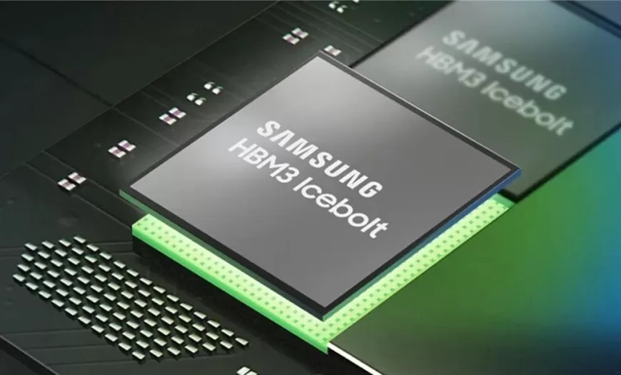
Samsung Electronics Co. is making significant strides in the competitive AI memory chip market, overcoming various setbacks. The tech giant has recently achieved notable progress, including gaining long-awaited approval from Nvidia Corp. for its high-bandwidth memory (HBM) chips, specifically the HBM3 version. Additionally, Samsung is on track to receive approval for the next generation, HBM3E, within the next few months.
These developments follow a series of challenges that allowed rival SK Hynix Inc. to take the lead in this rapidly growing sector. For South Korea's largest company, known for its dominance in the memory chip market, playing catch-up is an unusual experience. Historically, Samsung has leveraged its scale and engineering expertise to lead the way.
Although Samsung declined to comment on specific partnerships, the company stated that it is working closely with customers and that testing is proceeding smoothly.
Samsung’s recent achievements position it well to benefit from the surging demand for AI products. The HBM market is expected to grow significantly in the coming years. The sooner Samsung secures Nvidia's approval, the more it can capitalize on this increase.
Samsung is likely to face inquiries about its HBM strategy during its upcoming second-quarter earnings report. While the company aims to secure Nvidia’s approval by November, it continues to address various technical challenges associated with AI chips, which could potentially delay its timeline into 2025.
Samsung's recent struggles coincided with a challenging period for the company. Executive Chairman Jay Y. Lee faced legal battles over bribery and corruption allegations, during which senior leaders did not prioritize HBM development. The market only gained significant attention after the launch of AI applications, driving demand for Nvidia's AI model training chips.
While SK Hynix was prepared for this surge, Samsung faced engineering challenges with the new HBM chips. These chips consist of multiple DRAM layers stacked on top of each other, which generate substantial heat. When combined with Nvidia’s GPUs, which can reach high temperatures, proper heat dissipation becomes crucial.
Samsung uses a heat management technique called thermal compression non-conductive film (TC-NCF) to insulate each DRAM layer. Despite SK Hynix's alternative approach to improve heat dissipation, Samsung chose to enhance TC-NCF rather than switch methods. A spokesperson confirmed that TC-NCF is "well-proven technology" for future products.
Ultimately, Samsung modified its HBM design to address heating and power consumption issues, leading to Nvidia’s approval of HBM3. Jun Young-hyun, the new head of the semiconductor division, emphasized the company’s culture of collective problem-solving, stating that there have been "no issues related to heating and power consumption" in Samsung's HBM products and no design changes for specific customers.
Despite past missteps, Samsung's financial resources and production capacity provide a significant advantage. Once it meets Nvidia’s approval criteria, it can rapidly increase output, addressing current shortages.
Under Jun's leadership, Samsung has developed its own 12-layer HBM3E technology and is working to secure Nvidia's approval for both eight-layer and 12-layer versions.
As Samsung continues to advance, the market’s potential remains vast. Samsung's success in securing approvals and ramping up production will be crucial in determining its future position in the AI memory chip market.
Also Read: Apple Joins U.S. Effort for Responsible AI Use, White House Announces


